In this post, I want to give you a deep dive into PCB design for a capacitor load, created using Cadstar PCB design software. The focus here will be on crucial design aspects like temperature monitoring, voltage measurement, safety distances, and galvanically isolated current sensing. This design, intended for high-voltage DC applications, emphasizes proper spacing to meet UL standards and effective EMC shielding.
Temperature Monitoring for Capacitors and Power Resistors
When working with resistive loads and variable charging currents through capacitors, effective thermal management is critical. As seen in the upper-right section of the PCB layout, there are two dedicated connectors for temperature sensors, monitoring both power resistors and capacitors. These sensors are integrated using operational amplifiers in a Wheatstone Bridge configuration for differential temperature measurements.
Since temperature is captured via a differential measurement circuit, avoiding EMI (Electromagnetic Interference) from the capacitor's charging currents is essential. This was achieved by creating a shielded design, with a 5V polygon on the top layer and a ground polygon (GND) on the bottom layer, as depicted in the attached image.


Emergency Stop for DC Relays
The emergency stop mechanism in this design plays a critical role in safety, allowing immediate shutdown of all DC relays in case of a fault or overload. This feature protects both the system and the personnel working with it. The Schmitt trigger circuit, used to avoid unintended relay switching, is relatively immune to EMI issues. Additionally, clear silkscreen labels were added for ease of assembly, making sure the wiring is error-free and ensuring safety for the end user.

Current Sensing with Hall-Effect Sensor
For current measurement, we opted for the ACS758LCB-050B-PFF-T Hall-effect sensor due to its ability to provide galvanic isolation and meet the necessary clearance and creepage distances for high-voltage applications. The sensor's placement is shown in the PCB layout image, and it ensures accurate current measurement while maintaining electrical isolation.
The design mirrors the approach used for temperature sensing: a 5V polygon on the top layer and a GND polygon on the bottom layer. This reduces the chance of EMI coupling from surrounding high-current components. The sensor was added to the Cadstar component library, a process that will be detailed in a future blog post. The sensor is connected via a 3-pin header and custom-designed pads for easy integration.

Voltage Monitoring with Optocouplers
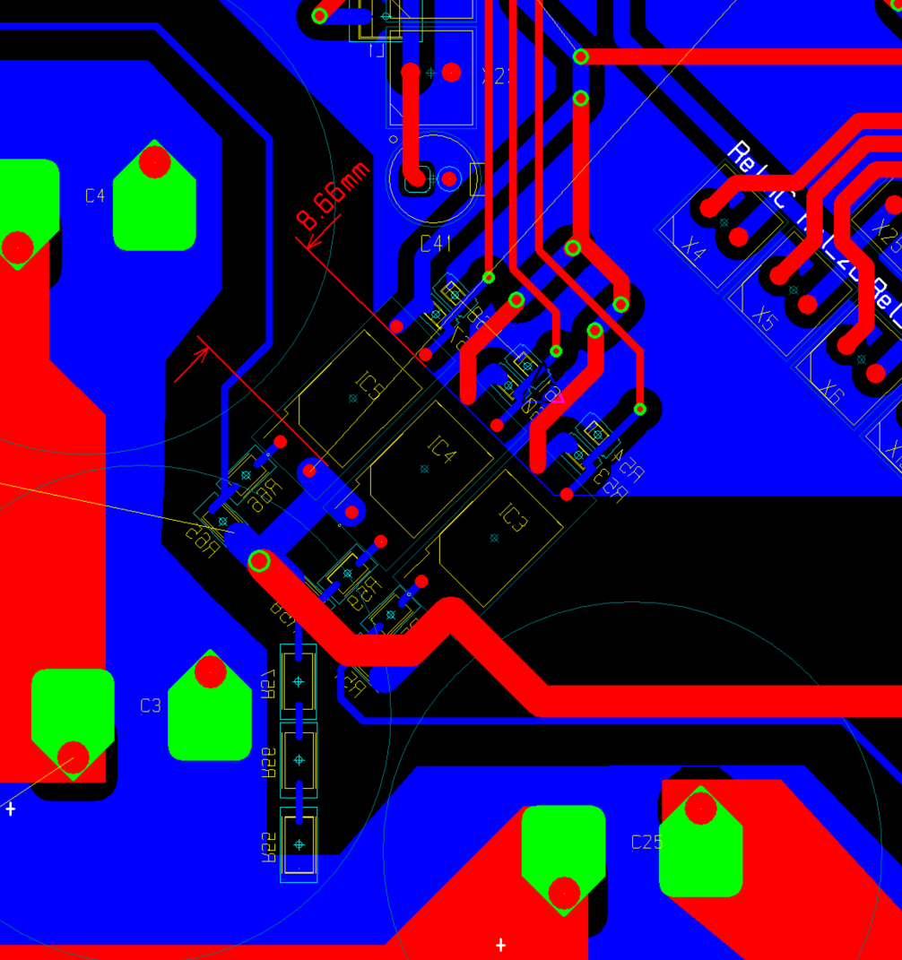
Voltage monitoring in this circuit is handled through three optocouplers paired with 1206 SMD resistors, each rated for 200V. The resistors are arranged in series to handle 830V, divided as 830V/2 = 415V, which falls well within the voltage tolerance. The circuit is referenced to PE (Protective Earth) to detect insulation faults. As per UL standards, a minimum clearance of 8 mm is required for circuits operating at 800V, and this design ensures a clearance of 8.66 mm.
The use of optocouplers guarantees safe voltage measurement while isolating the high-voltage section from the control electronics. I’ll dive into the calculation mistakes made during this phase and how they were corrected in a future post, so stay tuned for that.
Ground Plane Strategy and Filters
A properly designed ground plane is key to avoiding EMC issues. The ground plane in this design is large enough to ensure stable current flow, especially in the power section of the capacitors, which is labeled GND1 in the layout. This approach helps minimize ground loops and ensures low-impedance paths for return currents.
Several filter circuits were added to suppress high-frequency noise, including a small inductor for the fan power supply and a RC filter for the current sensing circuit. Especially in the high-power paths for the DC relays, it is critical to avoid ground loops that could lead to EMC disturbances.

Challenges in the Design Process
One of the biggest challenges was placing the capacitors and relays in the limited available space. As described in the circuit in the blog post "Building a Capacitive Load for a High-Voltage DC Network Test Station," large polygon pours were created to ensure an even current distribution and to meet the required current-carrying capacity. The tight layout constraints posed design challenges, as shown in the accompanying image.


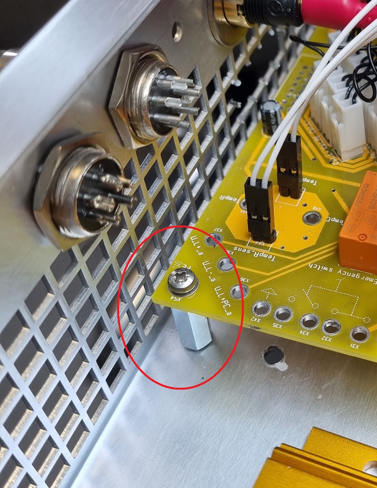
This unconventional method led to a critical oversight: no clearance rules were set for the relay contacts on the PCB's underside. As a result, Cadstar created GND1 polygons too close to the relay screw contacts, increasing the risk of electrical breakdown.

The quickest solution at that moment was to use plastic washers as insulation, as shown in the image. However, this temporary fix highlights the need for a more robust design review in future iterations.

One major challenge in this PCB design was finding space for additional power resistors needed for symmetry. As detailed in the article "Building a Capacitive Load for a High-Voltage DC Network Test Station", we had to select resistors that met the required power rating and value. Only the following resistors met the performance criteria and electrical specifications for this application.

Due to space constraints on the top side of the PCB—which was already filled with capacitors—we decided to place the additional power resistors on the bottom side of the board. This required the use of spacers and plastic standoffs, ensuring the PCB remained rigid and did not flex under pressure. These standoffs provided a 20mm clearance beneath the PCB to allow for safe installation of THT components like the TVS diodes, which would have required standoffs anyway.

Conclusion
That concludes this deep dive into the PCB design for the capacitor load. If you have any questions or suggestions on how to improve this Cadstar PCB design, feel free to leave a comment. I will cover topics like voltage calculation errors, component selection, and EMC mitigation techniques in future posts, so stay tuned!
Comments
Post a Comment